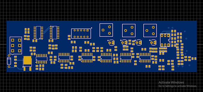
I will do kicad schematic, pcb design and gerber

India

I speak English
Established as a Proprietor firm in the year 2020, “Aastha Electronics Solutions” is a leading Manufacturer and Service Provider of a wide range of Electronic Cards, Circuit Boards, PCB assemblies, et...
About this Gig

I am an Electronics Engineer with around 4 years of hands-on knowledge of working on High-speed complex HDI designs.


I can Design Multi-layer PCB on any Tool which you prefer. I have the following skills in PCB layout designing


  • Schematic Designing 
  • HDI high-speed complex PCBs
  • PCBs with FPGA& ZYN, Processors, DDR3/4, PCIe, HDMI, Ethernet, USB 3
  • Designed Layout for 4G LTE, Wi-Fi Module, Bluetooth Antenna 
  • Differential signal and transmission line routing
  • Impedance calculation & Stack-up Building
  • RF PCBs with Rogers & FR-4 with complete impedance calculation of Transmission line
  • Digital & Analog(Mix signal PCBs)
  • Rigid and Flex PCBs
  • PCB in compliance with IPC Class III, IPC-A-600, IPC-A-610 & IPC-2220
  • Multi Stack boards enclosed in casings
  • Consultancy and technical support of PCB fabrication and assembly.
  • GERBER Generation 


Have been working on all these mentioned tools for over 4 years and designed them as per IPC Class III for military and IPC Class II for industrial usage.


Important Note: Please discuss your project and design requirements before placing an order so I have all the information about your project.
Specialization:

Circuit design

•

Schematics

•

Layout

•

Footprint

File format:

Gerber

•

SCH

•

3DS

•

PDF

Software:

Altium Designer

•

DipTrace

•

Eagle CAD

•

EasyEDA

•

KiCad

•

Matlab

Interface:

HDMI

•

I2S

•

UART

•

USB

•

SPI

•

I2C

•

Wi-Fi

•

BT

•

GSM/GPRS

•

LTE