Browse categories
Explore
Fiverr Pro
English
$
USD
ELECTRICAL AND ELECTRONICS ENGINEERING
Level 2
Has met high performance criteria and has a proven track record for meeting client expectations.
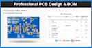
Are you looking for a professional PCB Designer who understands the supply chain specially for JLCPCB parts and LCSC?
Designing a PCB is only half the battle. If parts are out of stock or too expensive, your project stalls. I provide a "Complete BOM for JLCPCB parts assembly and LCSC" alongside PCB Design.
My Services:
Deliverables:
Why Choose Me? I engineer boards for performance, signal integrity, and thermal management. By managing the BOM and Sourcing during design, I prevent costly redesigns and ensure your project is "Production-Ready."
Message me with your requirements for a custom quote.


What files do I need to provide to get started?
Answer: To begin, I need your circuit schematic (PDF, Image, or CAD file) and a brief description of your project goals. If you have specific components you must use or a preferred board size, please let me know upfront.
Which software do you use for PCB Design?
Answer: I am proficient in Altium Designer, KiCad, and EasyEDA. I can provide the native source files for these platforms, allowing you to make future modifications easily. If you have a specific preference for your project, please let me know.
Can you find replacements for out-of-stock components?
Answer: Yes! I specialize in finding "Pin-to-Pin" compatible alternatives for chips that are currently out of stock or have long lead times. I will ensure the alternative matches the electrical specs and footprint of your original design.
Are your BOM files compatible with JLCPCB or PCBWay?
Answer: Absolutely. I format my Bill of Materials (BOM) and Pick & Place (CPL) files specifically to meet the requirements of major assembly houses like JLCPCB, PCBWay, and NextPCB to ensure a "one-click" upload experience for you.
Do you provide the source files for the PCB design?
Answer: Yes, depending on the package you select, I provide the full source files (Altium, KiCad, or EasyEDA) along with the standard manufacturing files (Gerber, NC Drill, and 3D STEP).
Can you help reduce the manufacturing cost of my current board?
Answer: Yes. I can perform a "BOM Scrub" and DFM (Design for Manufacturing) review to identify expensive components that can be replaced with more cost-effective equivalents without losing performance.
Do you perform Design for Manufacturing (DFM) checks?
Answer: Yes. Every design I deliver undergoes a thorough DFM check. I ensure that trace widths, clearances, and via sizes meet the specific capabilities of your chosen manufacturer (like JLCPCB’s 6mil/6mil rules) to prevent production errors and extra costs.
Can you handle multi-layer PCB designs?
Answer: Certainly. I have experience designing 2-layer, 4-layer, and 6-layer boards. For complex designs, I prioritize signal integrity, proper grounding (ground planes), and power distribution to ensure stable performance and EMI/EMC compliance.
What if I only have a hand-drawn sketch of my circuit?
Answer: That is no problem! I can perform Schematic Capture from your hand-drawn drawings or PDF sketches. I will create a professional, clean schematic and then proceed to the PCB layout and BOM generation.


