Browse categories
Explore
Fiverr Pro
English
$
USD
United States
Professional Electrical and electronics Engineer
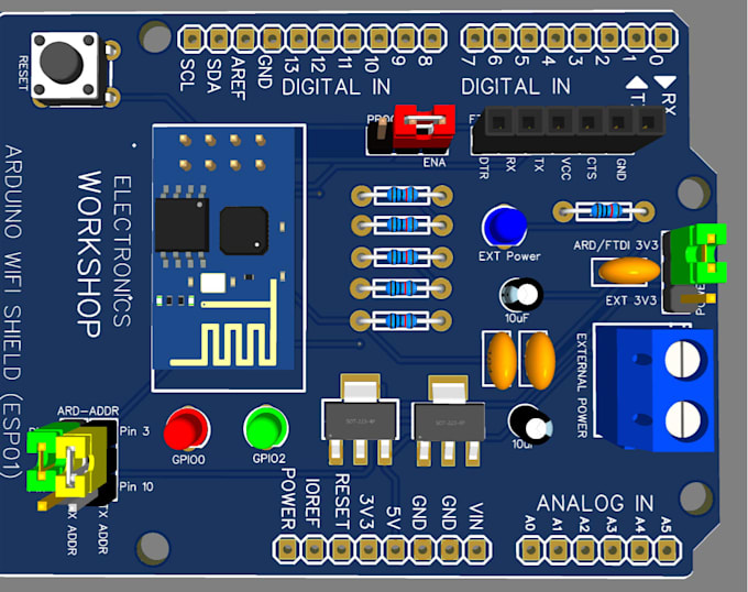
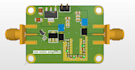
I WILL DESIGN ADVANCED IOT PCBS WITH WIRELESS CONNECTIVITY AND LOW POWER OPTIMIZATION
Welcome to my gig!
In this gig i am designing advanced iot pcbs with wireless connectivity and low power optimization.
a great IoT device starts with strong hardware. I design PCBs built for stable wireless links, clean power usage, and dependable sensor performance. Whether you're building a prototype or a product, I make sure your board is efficient and ready to scale.
What I Work On:
Ideal For:
Delivery Includes:
Lets build a board that performs well and stays efficient. CONTACT NOW to get started
#pcbdesign #layoutdesign #schematicdesign #gerberfile #pcbrouting #sensorintegration


Specialization:
Circuit design
•
Schematics
•
Layout
•
Footprint
•
Gerber
File format:
Gerber
•
STEP
•
VRML
•
3DS
•
Software:
Allegro
•
Altium Designer
•
Eagle CAD
•
EasyEDA
•
KiCad
•
Proteus
What format will the schematic be delivered in?
PDF, PNG, SVG, or the original design source files depending on your needs.
Do you redraw messy or outdated schematics?
Yes, I can digitize, clean, modernize, or fully redesign them.
Can you follow my exact component library?
Yes, I can use your library or create new custom symbols and footprints.
Do you support analog, digital, and mixed-signal circuits?
Yes, all types are supported.
Can you prepare a schematic for PCB production?
Yes, I format schematics specifically for PCB development and fabrication.