Browse categories
Explore
Fiverr Pro
English
$
USD
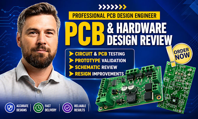
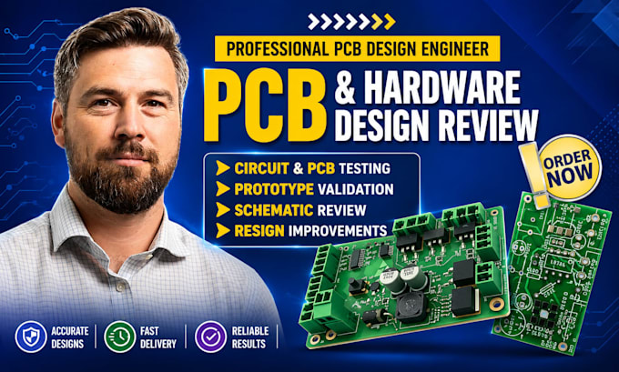
Electronics Engineer, PCB Design Expert, Altium, KiCad and EasyEDA PCB Designs
Hi there,
Looking for PCB review, PCB reverse engineering, Schematic Redesign, KiCad, Altium Designer, PCB Layout, Circuit Redesign, PCB Debugging, Gerber Review, BOM Verification, PCB Optimization, or an Electronics Engineer to help with accurate & production ready PCB solutions for reliable electronic products. Look no further.
I will review and optimize your PCB deslgn for manufacturing (DFM) to ensure it is fully production ready, cost effective, and free from common design flaws. Your deslgn will meet industry standards and be ready for fabrication.
What I Offer:
Tools I Use: Altium Designer, KiCad, Eagle or your preferred PCB design software
Requirement to Get Started: Your PCB Schematic file and/or PCB Layout file (Altium, KiCad, Eagle, or compatible format.
Why Choose Me:
Message Me Now And Let's Make Your PCB Design Error Free And Production Ready!


File format:
STEP
•
BRD
•
SCH
•
Software:
Altium Designer
•
EasyEDA
•
Fusion 360
•
KiCad
•
Proteus
•
Arduino
Interface:
HDMI
•
I2S
•
UART
•
USB
•
SPI
•
I2C
•
Wi-Fi
•
BLE
•
BT
•
GSM/GPRS
•
LTE
•
NB-IoT
Can you review my PCB design before I send it for manufacturing?
Yes. I perform a comprehensive PCB design review to identify layout errors, routing issues, DFM violations, signal integrity concerns, power distribution problems, and manufacturing risks before your board goes into production.
Can you reverse engineer an existing PCB and recreate the schematic?
Absolutely. I provide PCB reverse engineering services by recreating accurate schematics, PCB layouts, BOMs, and design files from an existing PCB, Gerber files, or reference board.
Do you work with Altium Designer, KiCad, Eagle, and EasyEDA?
Yes. I support Altium Designer, KiCad, Eagle, EasyEDA, and other industry-standard PCB design software. I can review, modify, optimize, or migrate your PCB project between supported platforms.
Can you debug and fix errors in my PCB layout or schematic?
Yes. I specialize in PCB debugging, schematic troubleshooting, circuit redesign, and PCB optimization. I can resolve routing conflicts, incorrect footprints, netlist errors, ERC/DRC violations, power issues, and component placement problems.
Can you verify my Gerber files and Bill of Materials (BOM) before fabrication?
Yes. I provide Gerber file review, BOM verification, footprint validation, Pick and Place file verification, and manufacturing checks to ensure your files are accurate and ready for PCB fabrication and assembly.
Will you optimize my PCB for better performance and lower manufacturing cost?
Yes. I optimize PCB layouts by improving component placement, trace routing, power and ground planes, thermal management, EMI/EMC performance, and overall Design for Manufacturability (DFM) to improve reliability while reducing production costs.
Can you redesign or upgrade an existing PCB without changing its functionality?
Yes. I can redesign an existing PCB, reduce board size, replace obsolete components, improve routing, upgrade the layout, and enhance manufacturability while preserving the original circuit functionality.
What files do you need to review or optimize my PCB design?
You can send your Altium Designer, KiCad, Eagle, EasyEDA, Gerber files, PCB layout files, schematics, BOM, PDFs, or manufacturing documents. I'll review the design, identify issues, and provide detailed recommendations or corrected production-ready files.