Browse categories
Explore
Fiverr Pro
English
$
USD
PCB EXPERT
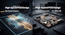
Are you facing signal issues, noise, or unstable performance in your high speed PCB design? High frequency circuits require precise layout techniques to avoid crosstalk, impedance mismatch, and data loss. I specialize in designing high speed PCBs that ensure signal integrity and reliable performance.
I will design professional high speed PCB layouts for RF, DDR, USB, and other high frequency applications with controlled impedance, differential pair routing, and optimized stackup. Every design is carefully structured to reduce noise, improve signal flow, and meet industry standards.
What you get includes high speed routing, impedance control, proper grounding techniques, EMI reduction strategies, and optimized layer stackup. I also ensure your PCB is ready for manufacturing with clean and accurate files.
I use tools like Altium Designer, KiCad, and EasyEDA to deliver precise results.
Perfect for engineers, startups, and advanced electronics projects. Message me before ordering to review your requirements and achieve the best performance.


Specialization:
Circuit design
•
Schematics
•
Layout
•
Gerber
File format:
Gerber
•
STEP
•
VRML
Software:
Cadence OrCAD
•
Eagle CAD
•
KiCad
•
CircuitMaker
Interface:
I2S
Can you fix signal integrity issues?
Yes, I analyze and optimize routing, grounding, and impedance.
Do you support RF and DDR designs?
Yes, including USB, HDMI, RF, and other high-speed interfaces.
Do you provide manufacturing files?
Yes, I deliver Gerber, BOM, and Pick & Place files.
Which tools do you use?
Altium Designer, KiCad, EasyEDA, and more


