Browse categories
Explore
Fiverr Pro
English
$
USD
Professional PCB Designer, Gerber and BOM
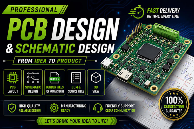
Are you looking for a professional PCB designer and electronics engineer to bring your circuit idea into reality? I will design high quality PCB layouts, schematic diagrams, and complete electronic circuit boards ready for prototyping and manufacturing.
I provide end-to-end PCB de=sign services using industry tools such as Altium Deslgner, KiCad, EasyEDA, and Eagle, ensuring precision, reliability, and production-ready output.
My expertise covers:
I focus on delivering clean, efficient, and error free de-signs that meet industry standards and ensure smooth production without issues.
Whether you are a startup, engineer, student, or inventor, I will help turn your electronic concept into a fully functional PCB product.
What types of PCB do you design?
I design single layer, double layer, multilayer, RF, high speed, and IoT PCB boards for various applications.
Do you offer revisions?
Yes, I provide revisions to ensure the final PCB design meets your exact requirements.
How fast can you deliver?
Delivery time depends on project complexity, but I also offer fast delivery for urgent PCB design tasks.
Can you optimize or fix my existing PCB design?
Yes, I can review, debug, and optimize your existing PCB layout or schematic to improve performance and reduce errors.
Is your PCB design ready for manufacturing?
Absolutely. I design production-ready PCB layouts optimized for fabrication at platforms like JLCPCB, PCBWay, and other manufacturers.
Do you design PCBs for ESP32, Arduino, or STM32?
Yes, I specialize in ESP32, Arduino, STM32, Raspberry Pi, IoT, and embedded system PCB designs.
Will I get Gerber files and BOM?
Yes. You will receive Gerber files, Bill of Materials (BOM), schematic files, and source project files ready for manufacturing.
Which software do you use for PCB design?
I use professional tools such as KiCad, Altium Designer, EasyEDA, and Eagle depending on project requirements.
Can you design PCB from just an idea?
Yes. I can convert your idea into a full circuit schematic and PCB layout including component selection, design optimization, and manufacturing files.
What do you need to start my PCB design?
I need a clear description of your project, circuit idea, schematic (if available), component list, and any reference files or sketches. If you don’t have details, I can help design from scratch.
