Browse categories
Explore
Fiverr Pro
English
$
USD
Professional PCB Layout Circuit Design Schematic Diagram Fast Delivery
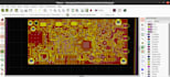
I will design your PCB using KiCad or EasyEDA, including professional PCB layout, component placement, routing, and design rule checking.
Whether you need a simple PCB or a more detailed multi-layer board, I can create a clean and organized design based on your schematic and requirements.
What I can provide:
PCB schematic and layout
Component placement and routing
Single and multi-layer PCB design
DRC check
Gerber and drill files
BOM (Bill of Materials)
PCB source/project files
3D PCB view
Software:
KiCad
EasyEDA
I focus on clean routing, proper component placement, and fabrication-ready files according to your requirements.
Please send your schematic, component list, board dimensions, and other PCB requirements before ordering. If your project is complex or doesn't fit a package, feel free to contact me for a custom offer.
Let's turn your circuit idea into a professional PCB design!


File format:
Gerber
Software:
EasyEDA
•
KiCad
•
LTspice
•
Matlab
•
Proteus
•
Arduino
Interface:
HDMI
•
USB
•
Wi-Fi
•
Ethernet
What do you need from me to start the PCB design?
Please provide your schematic or circuit diagram, component list/BOM if available, required board dimensions, number of layers, and any specific design or manufacturing requirements.
Which PCB design software do you use?
I primarily use KiCad and EasyEDA for schematic capture and PCB layout.
Can you design a PCB from my circuit schematic?
Yes. I can convert your provided schematic into a PCB layout with component placement, routing, and DRC checking.
Will I receive Gerber files?
Yes. Where included in your selected package, I can provide Gerber and drill files suitable for PCB fabrication, along with the relevant project/source files.
Can you design both single-layer and multi-layer PCBs?
Yes. I can work on single-layer and multi-layer PCB designs depending on the project requirements and selected package.
Can you create the PCB schematic too?
Yes. Schematic design can be included depending on the package. If you already have a schematic, I can focus on the PCB layout and routing.
Can you handle a PCB project that is not covered by your packages?
Yes. Send me your project requirements before ordering. For complex boards or projects with unusual requirements, I can discuss the scope and provide a custom offer.


