Browse categories
English
$
USD
Connect to your AI
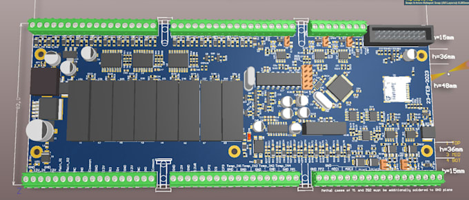
Power Electronics and PCB Design Expert
Looking for a professional PCB designer for your electronics project?
I provide PCB Design, PCB Layout, and Schematic Design services to help turn your electronic ideas into practical PCB solutions.
My Services:
What You Get:
Why Choose My Service?
Before Ordering:
Please share your circuit diagram, component list, board dimensions, and project requirements.
Contact me before ordering for complex or customized PCB projects. Let's bring your electronics project to life!
File format:
Gerber
•
STEP
•
SCH
•
•
Pcbdoc
Software:
Altium Designer
•
Cadence OrCAD
•
Eagle CAD
•
EasyEDA
•
KiCad
Interface:
UART
•
USB
•
SPI
•
I2C
•
CAT-M1
•
Ethernet
What information do you need to start PCB design?
I need your circuit diagram, component list, project requirements, and preferred PCB dimensions.
Do you provide Gerber files?
Yes, Gerber and drill files are available according to the selected package.
Can you design multilayer PCBs?
A: Yes, I can work on multilayer PCB designs depending on project complexity and agreed requirements.
Do you provide schematic diagrams and BOM?
A: Yes, schematic diagrams and Bill of Materials are included in the relevant packages.
Will I receive editable source files?
: Yes, editable project files are provided according to the selected package.
