Browse categories
Explore
Fiverr Pro
English
$
USD
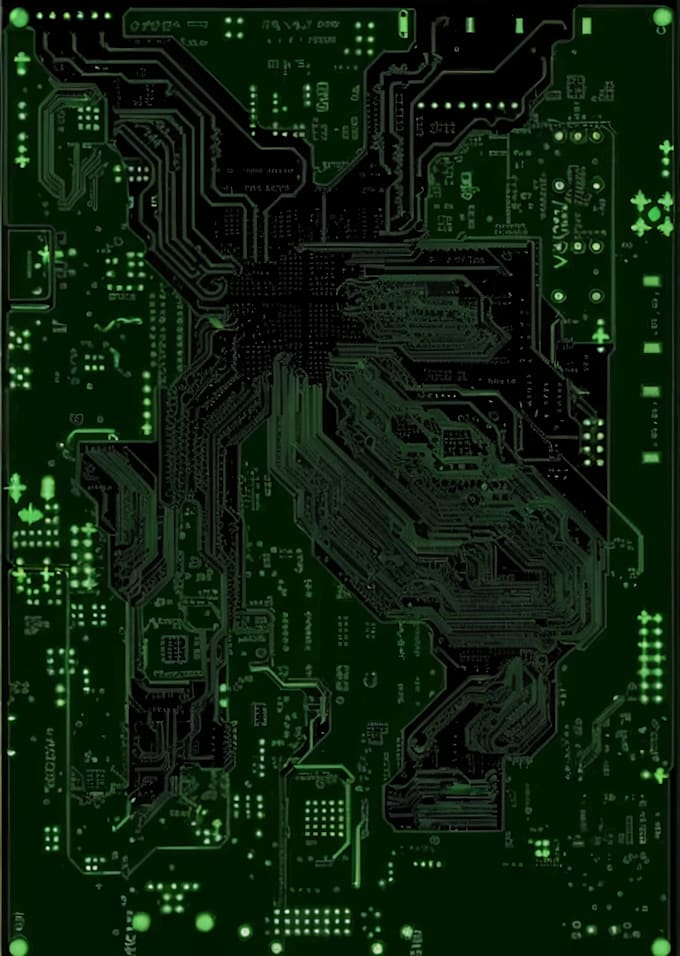
Power Electronics and PCB Design Expert
Looking for professional PCB layout
and routing in Altium Designer?
I will design your PCB schematic
and layout professionally for
embedded systems and FPGA boards.
What I offer:
- Multi layer PCB layout in Altium
- High speed routing and signals
- FPGA and Zynq board design
- Ethernet PHY and USB interfaces
- DDR memory routing and layout
- Gerber files for manufacturing
My expertise:
- Altium Designer PCB expert
- Cadence OrCAD schematics
- High speed signal integrity
- Power supply circuits
- Embedded systems boards
- DRC verified clean output
Why choose me:
- Professional Altium expert
- Manufacturing ready output
- Fast delivery with revisions
- Clear communication
Send requirements and get
professional PCB delivered fast.
Order now!


Specialization:
Circuit design
•
Schematics
•
Layout
•
Footprint
•
Gerber
File format:
Gerber
•
SCH
•
•
ODB
Software:
Altium Designer
•
Cadence OrCAD
•
KiCad
Interface:
UART
•
USB
•
SPI
•
I2C
•
SDIO
•
Ethernet
What software do you use for PCB design?
I use Altium Designer as my primary tool for professional PCB layout and routing. I also work with Cadence OrCAD and KiCad.
What files will I receive after ordering?
You will receive complete Altium project files Gerber files PDF schematic Bill of Materials and 3D STEP model based on your package.
Can you design high speed PCB with DDR and Ethernet?
Yes I have experience designing high speed PCB layouts including DDR memory routing Gigabit Ethernet PHY FPGA boards and USB interfaces.
How many layers can you design?
I can design 2 layer to 6 layer PCB boards depending on your requirements and selected package.
Will the PCB be ready for manufacturing?
Yes Standard and Premium packages include complete Gerber files verified with DRC and ready to send directly to manufacturer.