Browse categories
Explore
Fiverr Pro
English
$
USD
Custom PCB and RF Solutions, Altium, KiCad, Schematic, PCB Layout
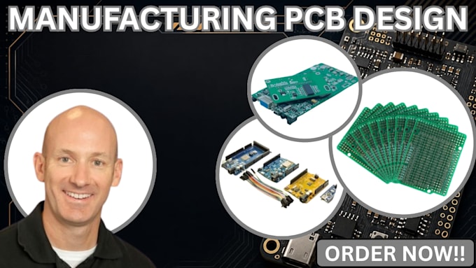
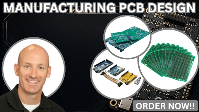
Looking for a reliable PCB designer for your IoT, Arduino, or electronics project?
I will create professional printed circuit board prototypes, IoT PCBs, multilayer PCBs, and Arduino PCBs using KiCad. Whether you have a schematic, circuit diagram, reference design, or project concept, I can help turn your requirements into a clean and organized PCB layout.
MY SERVICES INCLUDE:
SOFTWARE
KiCad
I focus on clean layouts, proper component placement, organized routing, and manufacturing requirements to help make your PCB ready for prototyping or production.
Whether you are building an Arduino project, IoT device, sensor system, embedded controller, or custom electronic product, send me your requirements and I will review the project before starting.
CONTACT ME NOW!!
File format:
Gerber
•
STEP
•
BRD
•
SCH
•
Software:
Altium Designer
•
Eagle CAD
•
EasyEDA
•
KiCad
Interface:
HDMI
•
UART
•
USB
•
I2C
•
Wi-Fi
•
BLE
•
BT
•
Ethernet
Can you design Arduino PCBs?
Yes. I can create custom Arduino based PCB layouts according to your schematic and project requirements.
Do you design IoT PCBs?
Yes. I can work on IoT boards using platforms such as ESP32, ESP8266, Arduino, and other embedded controllers.
Can you create multilayer PCBs?
Yes. I can work with multilayer PCB layouts depending on the board complexity and requirements.
Do you use KiCad?
Yes. KiCad is the primary software used for this service.
Can you convert my schematic into a PCB?
Yes. Send your schematic and component information, and I can develop the PCB layout.
Do you provide Gerber files?
Yes. Gerber and other manufacturing outputs can be provided according to the selected package.
Can you modify an existing KiCad PCB?
Yes. You can send your existing KiCad project files and describe the modifications required.
Can you design a PCB for manufacturing?
Yes. I can prepare manufacturing-ready files such as Gerbers, drill files, BOM, and Pick & Place files when required.
Please provide the following when available:
Project description Schematic or circuit diagram BOM/component list Component datasheets Required PCB dimensions Number of layers Board outline Mounting-hole locations Input/output voltage requirements Current requirements Connector locations Arduino/ESP/STM32 specifications, if applicable