Browse categories
Explore
Fiverr Pro
English
$
USD
PCB Designer and Hardware Engineer
You have a hardware idea but turning it into a real, working PCB is where things get complicated. That's where I come in.
I'm Alaeddine, an Electrical & Computer Engineer based in Berlin. I design PCBs that are clean, well-documented, and ready to send straight to your fab house working exclusively in Altium Designer.
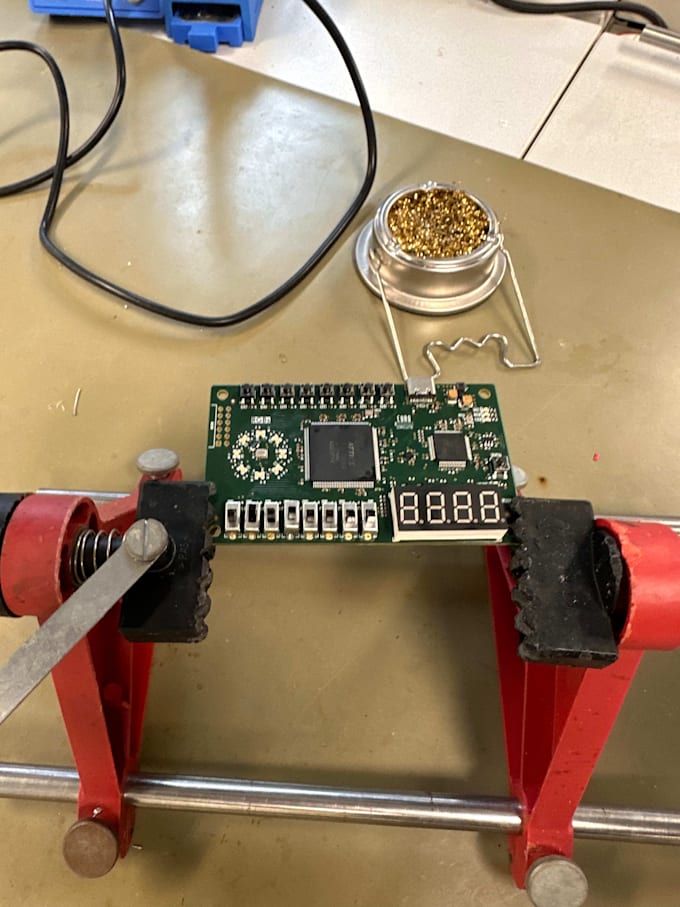
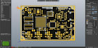
My work includes a 4-layer FPGA development board (Lattice MachXO2, FT2232H, MEMS microphone, accelerometer) built for my bachelor's thesis, and a 10-layer high-speed board with DDR interfaces, Gigabit Ethernet, and full PDN analysis.
What I offer: Schematic capture · PCB layout (2-10 layers) · FPGA board design · Custom symbols & IPC-compliant footprints · Gerbers, BOM & fabrication notes
I don't just move traces I understand why each decision matters and explain it to you. Clear communication, no surprises, and I won't close the project until you're satisfied.
Not sure which package fits? Message me I'm happy to talk through your project before you commit.


Specialization:
Circuit design
•
Schematics
•
Layout
•
Footprint
•
Gerber
File format:
Gerber
•
STEP
•
SCH
•
•
ODB
Software:
Altium Designer
•
LTspice