Browse categories
Explore
Fiverr Pro
English
$
USD
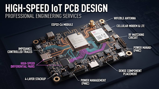
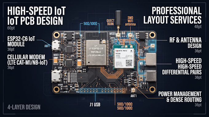
High Speed IoT PCB Design with ESP32-C6, Cellular Modem and RF Layout
Wireless IoT hardware combines several sensitive design areas, including high speed digital interfaces, RF transmission lines, cellular communication and power management.
I develop high speed IoT PCBs using ESP32-C6, cellular modems and RF layout techniques for connected devices, tracking systems, industrial sensors and smart embedded products. I focus on clean routing, controlled return paths, effective grounding and practical manufacturing requirements.
What I offer:
What you will get:
Contact me with your schematic, modem details and board specifications to get started.
File format:
Gerber
•
STEP
•
VRML
•
3DS
•
Software:
Allegro
•
DipTrace
•
Eagle CAD
•
EasyEDA
•
LTspice
•
Arduino
Interface:
MIPI DSI/CSI
•
I2S
•
UART
•
USB
•
SPI
•
I2C
•
PCIe
•
Wi-Fi
•
BT
•
LTE
Can you integrate a cellular modem with ESP32-C6?
Yes. I can connect the modem through UART, USB or another interface specified by your system architecture.
2. Do you design high speed PCB traces?
Yes. I can route high speed interfaces with attention to impedance, trace spacing, return paths and signal integrity.
Can you handle both WiFi and cellular RF layout?
Yes. I can work on WiFi and cellular antenna regions, RF routing, grounding and matching network placement.
Do you provide a 4 layer PCB design?
Yes. I can develop 4-layer boards with appropriate power, signal and ground layer planning.
5. Can you prepare files for JLCPCB?
Yes. I can provide Gerbers, drill files, BOM, pick-and-place files and other required manufacturing outputs.