Browse categories
Explore
Fiverr Pro
English
$
USD
Python Developer, MATLAB and PCB Design Engineer
Having trouble turning your circuit idea into a proper PCB?
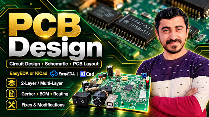
I can help you design, fix, or improve your circuit and turn it into a clean PCB layout using EasyEDA or KiCad.
If you have an incomplete schematic, messy routing, wrong component placement, or you are not sure how to prepare your PCB for manufacturing, I can help you solve it.
I can work from your:
I can help with:
My goal is to make the design clean, practical, and ready for manufacturing.
If your project is complex or has special requirements, please message me before placing the order so I can review the details first.
Send me your circuit or project idea and I will help you turn it into a complete PCB design.

What do you need to start my PCB design project?
Please provide your project requirements, circuit diagram, schematic (if available), PCB dimensions, preferred software, and any specific design instructions.
Which PCB design software do you use?
I work with Altium Designer, KiCad, Eagle, and EasyEDA. If you have a preferred software, let me know before we begin.
