Browse categories
Explore
Fiverr Pro
English
$
USD
Need a reliable PCB that bridges sensors, microcontrollers, and real-world signals? I design clean, professional 2-layer PCBs for embedded and IoT projects from schematic capture to fully routed, manufacturable boards.
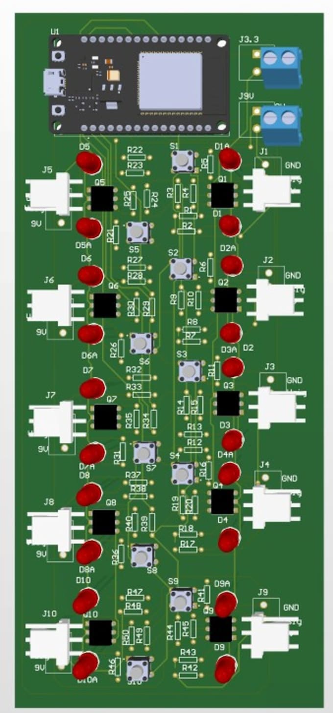
As a portfolio example, I've designed a 10-channel analog interface PCB built around an ESP32, using optocoupler-isolated inputs (4N35), voltage attenuation, and buffered signal paths to safely convert 9V sensor signals down to 3.3V logic levels for stable microcontroller interrupt triggering. This is shown in my gig gallery as proof of the quality and complexity I work at.
What I offer:
Schematic capture
multi-layer PCB layout and routing
Signal conditioning circuits (voltage dividers, buffers, optocouplers, relays)
Microcontroller integration (ESP32, Arduino, STM32, and more)
Component footprint selection & BOM (Bill of Materials) preparation
Design for Manufacturing (DFM) checks
Gerber, drill, and pick-and-place files ready for fabrication
Why work with me: