Browse categories
Explore
Fiverr Pro
English
$
USD
Turning Electronics Concepts Into Production Ready PCB Designs
Need a clean, professional PCB design for your electronics project?
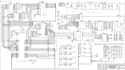
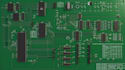
I will design your PCB layout and circuit schematic using KiCad, based on your schematic, circuit diagram, component list, datasheets, or project requirements.
My services include:
I can work on prototypes, embedded electronics, IoT devices, sensor boards, microcontroller projects, control boards, and other custom PCB applications.
My focus is on organized schematics, practical component placement, clean routing, and properly prepared project files.
Please send your circuit information, component list, dimensions, reference files, or requirements before ordering so I can confirm the project scope and recommend the appropriate package.
Let's turn your electronics idea into a clean KiCad PCB design ready for the next stage.
File format:
STEP
•
SCH
•
3DS
•
•
ODB
Software:
Allegro
•
Altium Designer
•
Eagle CAD
•
EasyEDA
•
KiCad
•
Matlab
Interface:
HDMI
•
MIPI DSI/CSI
•
TDM
•
UART
•
USB
•
SPI
Can you design a PCB from my schematic?
Yes. Send your schematic, circuit diagram, component list, or reference design and I can create the PCB layout in KiCad.
Can you create the schematic as well?
Yes. I can create or modify the circuit schematic depending on your project requirements and the information provided.
Do you provide Gerber files?
Yes. Gerber and drill files can be included in the appropriate package.
Do I receive the editable KiCad files?
Yes. Editable KiCad project files can be included according to the selected package.
Can you create custom footprints?
Yes, custom footprints can be created when an appropriate existing footprint is not available.
Can you design 2-layer and 4-layer PCBs?
Yes, depending on the project complexity and selected package.
Can you design PCB layouts from an existing schematic?
Yes. You can provide your existing schematic and I can develop the PCB layout, component placement and routing from it.
Can you work with ESP32, Arduino or STM32 projects?
Yes, provided you supply the relevant circuit requirements, components, reference designs and specifications.
Can you provide manufacturing-ready files?
Yes. Depending on the package, I can provide Gerber, drill, BOM and other required manufacturing-related files.
Should I contact you before ordering?
Yes. For complex, high-speed, RF, multi-layer, power or unusual designs, contacting me first allows us to confirm the scope and requirements.


