Browse categories
Explore
Fiverr Pro
English
$
USD
RF and Microwave Antenna and PCB Designer, Electronics Engineer
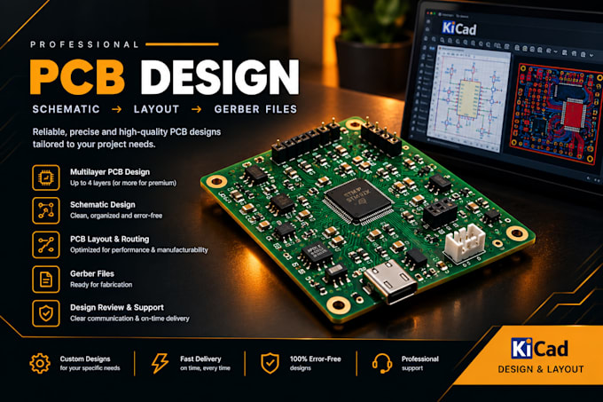
Looking for a professional PCB design for your electronic project? I can transform your circuit ideas, schematics, or concepts into organized PCB layouts using KiCad.
My Services Include:
Single-layer, double-layer, and multilayer PCB design (up to 4 layers)
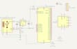
Schematic design and schematic-to-PCB conversion
Component placement and track routing
Design Rule Check (DRC)
Gerber and drill file generation
Bill of Materials (BOM)
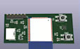
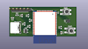
3D PCB visualization
Existing PCB modifications and improvements
What You'll Receive:
Depending on your selected package, deliverables may include KiCad project files, schematics, Gerber and drill files, a BOM, and a 3D PCB view.
I focus on clean layouts, organized routing, appropriate component footprints, design-rule compliance, and clear communication to meet your project requirements.
Please contact me before ordering to discuss your circuit, component count, board dimensions, layer requirements, and deliverables.
File format:
Gerber
•
Software:
KiCad
Interface:
UART
•
USB
•
SPI
•
I2C
What information do you need to start a PCB design?
Please share your circuit schematic, project requirements, component list (if available), board dimensions, and preferred layer count. If you only have an idea, contact me to discuss your requirements.
Which software do you use for PCB design?
I use KiCad for schematic design, PCB layout, component placement, routing, design rule checks, and manufacturing file preparation.
Do you design PCBs with up to 4 layers?
Yes, I offer single-layer, double-layer, and up to 4-layer PCB layouts, depending on project complexity. Please contact me before ordering complex multilayer designs.
Will you provide Gerber files for PCB manufacturing?
Yes, Gerber and drill files are available according to your selected package, along with the relevant KiCad project files when included.
Do you provide schematic design and PCB layout together?
Yes, I can create a schematic and convert it into a PCB layout. If you already have a schematic, I can work from your existing design.
Can you provide a Bill of Materials (BOM)?
Yes, a BOM containing component references, values, and available part information can be included, depending on your selected package.
Do you provide a 3D view of the PCB?
Yes, I can provide a 3D PCB visualization where suitable component footprints and 3D models are available. This depends on your selected package.
Can you modify an existing PCB design?
Yes, I can help modify existing PCB layouts, adjust component placement, improve routing, and update board dimensions according to your requirements.
Will my PCB be ready for manufacturing?
I can prepare manufacturing files according to your specified requirements and check the design rules. Final fabrication suitability depends on the manufacturer's specifications and appropriate design verification.
Should I contact you before placing an order?
Yes, please contact me for complex circuits, multilayer boards, or special requirements so we can confirm the scope, deliverables, and timeline before starting.