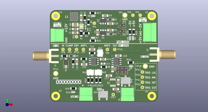
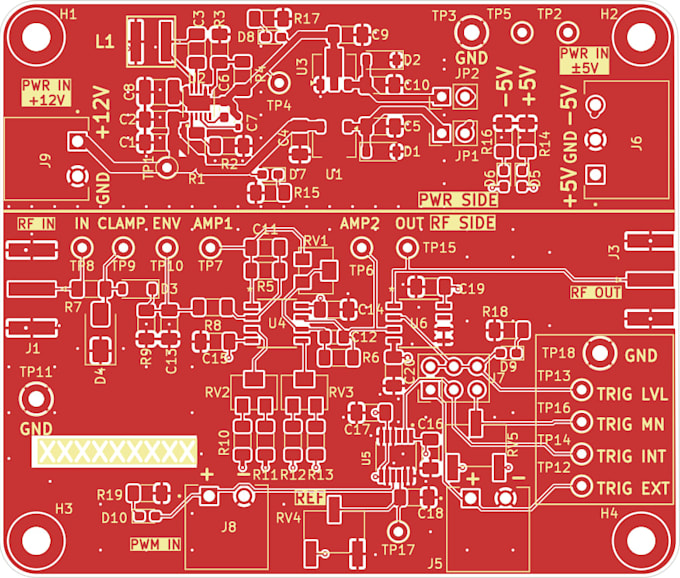
I will design rf pcb layout, antenna integration and high frequency rf circuits

United States

I speak English, German, Italian

RF PCB layout, antenna design, impedance control and wireless PCB solutions

I’m a professional PCB designer specializing in RF PCB, high frequency PCB layout, antenna integration, controlled impedance routing, and wireless electronics. My services include schematic capture,...
About this Gig

Are you looking for reliable RF PCB, high-frequency circuit development, or antenna integration for your electronic project?


I will design RF PCB layouts and high-frequency RF circuits for wireless communication, IoT devices, and advanced electronic systems.


My services include:

  • RF PCB design and high-frequency PCB layout
  • RF schematic design and circuit development
  • Antenna design and PCB antenna integration
  • Impedance matching networks and RF optimization
  • 50-ohm controlled impedance routing
  • WiFi, Bluetooth, BLE, LoRa, GPS, GNSS, and 5G RF PCB
  • RF amplifier, transmitter, and receiver circuit design
  • RF simulation and electromagnetic analysis using HFSS, CST, and other suitable tools
  • PCB layout optimization, grounding, shielding, and signal integrity
  • Manufacturing-ready Gerber files, BOM, and design documentation


I work with KiCad and Altium Designer to develop practical RF PCB solutions with attention to impedance control, signal integrity, antenna performance, grounding, and manufacturability.


Please contact me before placing an order
Specialization:

Circuit design

•

Schematics

•

Layout

•

Simulations

File format:

Gerber

•

STEP

•

BRD

•

SCH

•

PDF

Software:

Altium Designer

•

Eagle CAD

•

EasyEDA

•

KiCad

Interface:

UART

•

USB

•

SPI

•

I2C

•

SDIO

•

PCIe

•

Wi-Fi

•

BLE

•

BT

•

GSM/GPRS

•

LTE

•

CAT-M1