Browse categories
Explore
Fiverr Pro
English
$
USD
PCB Design Engineer delivering reliable, manufacturing ready hardware systems
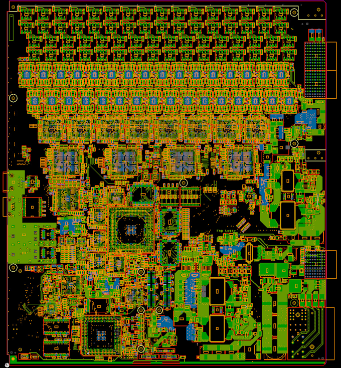
PCB layout design for embedded and electronic hardware, developed from defined schematics and system requirements.
The layout process follows controlled placement and routing, with verification through DRC. Design decisions consider signal integrity, power distribution, grounding strategy, and stackup configuration where applicable.
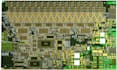
Applied to multilayer boards and microcontroller-based systems including ESP32 and STM32 platforms.
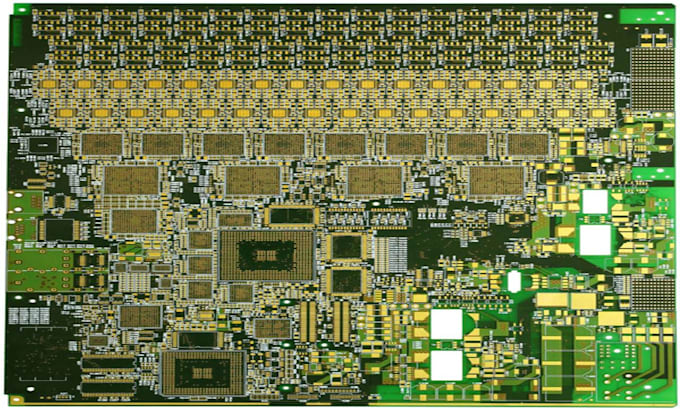
Manufacturing outputs are provided in standard formats: Gerber, drill data, and BOM, aligned with fabrication and assembly requirements.
Execution is based on actual constraints such as layer count, routing density, and board complexity.