Browse categories
English
$
USD
Connect to your AI
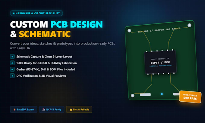
Looking to turn your circuit idea, breadboard prototype, or hand-drawn sketch into a clean, working PCB? You're in the right place!
I provide professional schematic capture and PCB layout design using EasyEDA, fully prepared for smooth fabrication at JLCPCB or PCBWay.
What I can do for you:
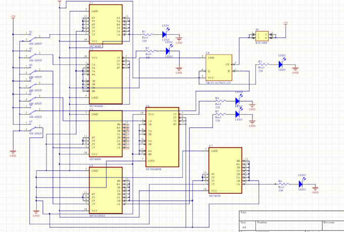
- Convert your rough sketch, breadboard, or circuit diagram into a clean schematic
- Design clean 2-layer PCB layouts with proper ground planes & trace routing
- Component placement & standard footprint assignment
- Design Rule Check (DRC) to ensure 100% manufacturing readiness
What you will receive:
- EasyEDA project source files
- Gerber files (RS-274X) ready for JLCPCB / PCBWay fabrication
- Drill files (Excellon)
- Bill of Materials (BOM) in CSV/Excel
- 3D visual preview of your board (PNG/PDF)
Why choose this service?
- Clear communication and fast turnaround
- Accurate, production-ready files
- Free consultation before ordering
Have questions or a custom circuit requirement?
Feel free to contact me before placing an order so we can discuss your project!
Specialization:
Circuit design
•
Schematics
File format:
Gerber
•
•
Other
Software:
EasyEDA
Interface:
UART
•
USB
•
SPI
•
I2C
•
Wi-Fi
•
BLE
•
BT
What information do you need from me to get started?
You can provide a circuit diagram, a hand-drawn sketch, a photo of your breadboard prototype, or a list of components along with an explanation of how they should be connected.
Do you manufacture and ship the physical PCB?
No, this service provides digital production-ready files (Gerber, Drill, BOM). You can directly upload these files to JLCPCB, PCBWay, or any manufacturer of your choice to get your physical boards produced.
What software do you use for design?
I use EasyEDA, which is fully compatible with JLCPCB and standard PCB fabrication houses worldwide.