Browse categories
Explore
Fiverr Pro
English
$
USD
PCB DESIGN AND FIRMWARE DEVELOPMENT
HELLO AND WELCOME BUYER!!
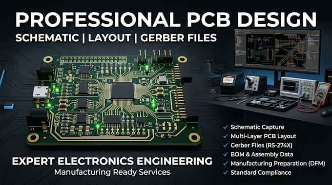
A successful electronic product starts with a well engineered schematic and an optimized PCB layout. Every trace, component placement and routing decision directly affects performance, reliability, manufacturability, and production cost. I design professional PCBs using industry standard engineering practices to ensure your hardware is ready for prototyping and mass production.
Whether you are developing an IoT device, embedded system, industrial controller, power supply or consumer electronics product, I will transform your concept into a complete hardware design package with accurate schematics, optimized PCB layouts, and manufacturing ready Gerber files.
Service Included:
Electronic schematic design
Professional PCB layout design
Single, double, and multilayer PCBs
Component selection
High speed and differential signal routing
Why Choose Me:
Share your project details today, and I'll deliver a professional PCB design package ready for manufacturing and assembly
Specialization:
Circuit design
•
Schematics
•
Layout
•
Analysis
•
Gerber
File format:
Gerber
•
SCH
•
Software:
Allegro
•
Altium Designer
•
Cadence OrCAD
•
EasyEDA
•
KiCad
Interface:
UART
•
USB
•
Wi-Fi
•
BT
•
LTE
Which PCB design software do you use?
I work with KiCad, Altium Designer, EasyEDA, Autodesk Eagle, and other industry standard PCB design tools.
Will I receive manufacturing ready files?
Yes. You'll receive Gerber files, NC Drill files, BOM, Pick and Place files, PDFs, and all documentation required for PCB manufacturing and assembly.
Can you create a PCB from my circuit idea or block diagram?
Yes. I can design the complete schematic, PCB layout, and manufacturing files from your concept, specifications, or reference materials.
Do you design multilayer and high speed PCBs?
Yes. I design 2 layer, 4 layer, 6 layer, and higher multilayer PCBs with proper impedance control, signal integrity, and power distribution.
Can you improve or redesign an existing PCB?
Absolutely. I can optimize layouts, fix routing issues, improve manufacturability, reduce EMI, and prepare your design for production.