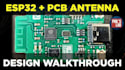
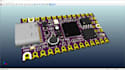
ESP32 PCB Design | Multilayer Schematics, Layout & KiCad Expertise
I design professional PCBs specifically for ESP32 and embedded IoT projects. Complete schematic design in KiCad, optimized multilayer layouts, and production-ready files, all tailored for your IoT application.
- What's Included:
- Complete schematic design in KiCad (well-organized, properly annotated)
- Power distribution & voltage regulation design
- USB/Serial programming interface
- Wireless antenna design (WiFi/Bluetooth optimization)
- Multi-layer PCB layout (2-4 layers optimized for signal integrity)
- Proper trace routing & impedance control
- Component placement for manufacturability & thermal performance
- 3D STEP model (mechanical fit-check)
- Gerber files + NC drill files (production-ready)
- Bill of Materials (BOM) with part numbers
- Assembly documentation & layer stackup
- Design for Manufacturing (DFM) review
Ready to bring your ESP32 project to life? Message me your details first!