Browse categories
Explore
Fiverr Pro
English
$
USD
Professional PCB Design for KiCad, EasyEDA, BMS and Embedded Electronics
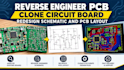
Do you have an existing PCB that needs to be recreated, documented or redesigned?
I will reverse engineer your PCB and recreate the schematic and PCB layout for development or manufacturing purposes.
I can work from clear PCB photographs, existing board files, available schematics, component information or a physical board where appropriate. The process can include identifying components, tracing connections, recreating the schematic, assigning footprints, rebuilding the PCB layout and preparing manufacturing outputs.
If your existing board has design limitations, I can also help redesign and optimize the layout while maintaining the required electrical functionality. This may include improved component placement, routing cleanup, power and ground organization, footprint corrections, connector changes and design-for-manufacturing improvements.
Depending on the package, deliverables can include recreated schematic, PCB layout, BOM, Gerber files, drill files, Pick & Place/CPL, assembly documentation, 3D PCB model and editable source files.
This service is useful for obsolete boards, unavailable source files, prototype recreation, legacy hardware documentation
Message now

Can you reverse engineer a PCB from photos?
Yes, clear high-resolution images of both sides can be used for suitable boards.
Can you recreate the schematic?
Yes. Schematic recreation can be included depending on the board complexity.
Can you recreate the PCB layout?
Yes, the PCB can be reconstructed in the agreed software.
Can you redesign the board after reverse engineering?
Yes. Standard and Premium packages can include redesign and optimization.
Can you provide Gerbers?
Yes, manufacturing outputs can be included.
