Browse categories
Explore
Fiverr Pro
English
$
USD
PCB Design Engineer
HELLO GREAT BUYER WELCOME TO MY GIG !!!
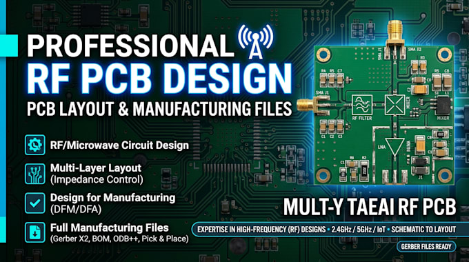
Are you looking for a reliable RF PCB for your electronic product?
I help engineers, startups, and businesses create high performance RF PCBs ready for fabrication and assembly. Every PCB is optimized for signal integrity, efficiency, and manufacturing.
What I Offer:
Why Choose Me:
Tools I Use:
Perfect for wireless devices, IoT products, embedded systems, RF modules, and custom electronic hardware.
Message me today and get a professional RF PCB with complete manufacturing files ready for production.
Can you create RF PCBs from scratch?
Yes, I can develop the schematic, PCB layout, and production files based on your specifications.
Do you provide manufacturing files?
Yes, I provide Gerber, BOM, Pick and Place files, and assembly documentation.
Can you work on multilayer RF boards?
Yes, I support 2-layer, 4-layer, and advanced multilayer PCBs.
Will the PCB be ready for fabrication?
Yes, every project is delivered with production-ready files.