Browse categories
English
$
USD
Connect to your AI
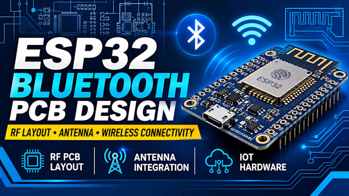
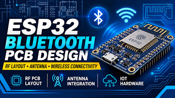
ESP32 PCB Designer RF Layout Wireless Hardware Specialist
Are you looking for a custom ESP32 PCB for your Bluetooth, WiFi, or IoT project?
I provide professional PCB design solutions for startups, electronics developers, engineers, and hardware innovators looking to turn their ideas into functional circuit board designs. I can design custom ESP32 PCBs, develop circuit schematics, integrate Bluetooth and WiFi modules, handle RF layout, antenna integration, component placement, and impedance-controlled routing.
Whether you are building a wireless sensor, smart device, automation system, or connected IoT product, I focus on clean PCB layouts, reliable component integration, signal integrity, and design requirements specific to your application.
I work with KiCad, Altium Designer, and EasyEDA to deliver organized, manufacturing-ready design files, including Gerber, BOM, drill files, and editable project files.
Share your project requirements, sketches, or existing schematics, and I will help develop a PCB design suited to your product.
Let's bring your wireless electronics project to life!
Specialization:
Circuit design
•
Layout
•
Footprint
•
Simulations
•
Gerber
File format:
Gerber
•
STEP
•
BRD
•
•
PDSPrj
Software:
Allegro
•
EasyEDA
•
Fusion 360
•
NI Multisim
•
Simulink
•
AutoCAD