Browse categories
Explore
Fiverr Pro
English
$
USD
RF Filter & Amplifier PCB Layout for Radios & Wireless Modules
Looking for a high-performance RF PCB layout for your radio or wireless project? You're in the right place!
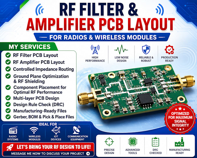
I specialize in designing RF filter and amplifier PCB layouts optimized for signal integrity, impedance control, low noise, and reliable performance. Whether you're developing RF modules, wireless communication devices, IoT products, or custom radio systems, I deliver production-ready PCB designs tailored to your requirements.
My services include:
I work with industry-standard PCB design tools and follow best practices to ensure excellent RF performance and manufacturability.
Let's turn your RF concept into a reliable, high-quality PCB design. Feel free to contact me before placing your order to discuss your project.


What software do you use for RF PCB layout?
I work with Altium Designer, KiCad, and Eagle. If you have a preferred tool, just let me know and I'll match it.
Do I need to provide a schematic before starting?
Yes, a completed schematic (with component values and RF specs) is needed to begin. If you don't have one yet, I can also help with schematic capture as an add-on.
Can you match my board to a specific impedance?
Yes, impedance-controlled routing is part of my standard process, including trace width calculations based on your PCB stack-up and material.
What stack-up or PCB material do you recommend for RF designs?
It depends on frequency and application. I typically recommend low-loss materials like Rogers or FR4 with proper stack-up planning, and I'll advise based on your specific project.