Browse categories
Explore
Fiverr Pro
English
$
USD
Need a PCB designed for your circuit or project?
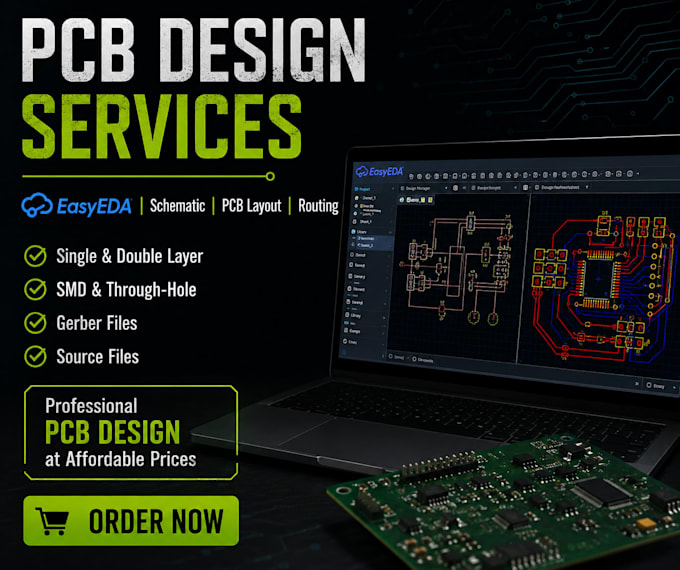
I can design a PCB schematic and layout in EasyEDA based on your circuit diagram, requirements, or reference design.
What I can help with:
I can work with your existing schematic or help convert your circuit into a PCB.
I focus on clean layouts, proper connections, and organized designs. Before placing an order, please send your circuit diagram, component list, board requirements, and any specific dimensions or constraints.
If you are not sure which package you need, feel free to contact me with your project details.

File format:
Gerber
•
VRML
•
BRD
•
•
SLX
Software:
EasyEDA
•
Proteus
Interface:
UART
•
I2C
•
Wi-Fi
•
LTE
What do you need from me to start the PCB design?
Please provide your circuit diagram or schematic, component list, board dimensions, preferred components, and any specific requirements you have.
Which software do you use for PCB design?
I primarily use EasyEDA for schematic design and PCB layout.
Can you design a PCB from a circuit diagram?
Yes. You can send me your circuit diagram, and I can create the schematic and PCB layout based on it.
Do you provide Gerber files?
Yes. Gerber files are included in the every package.
Can you work with SMD and through-hole components?
Yes, I can design PCBs using both SMD and through-hole components, depending on the project requirements.
Do you provide the EasyEDA source files?
Yes. The EasyEDA project/source files are included with the packages where specified.
Can you design both single-layer and double-layer PCBs?
Yes. I can design single-layer and double-layer PCB layouts depending on the requirements of your project.
