Browse categories
Explore
Fiverr Pro
English
$
USD
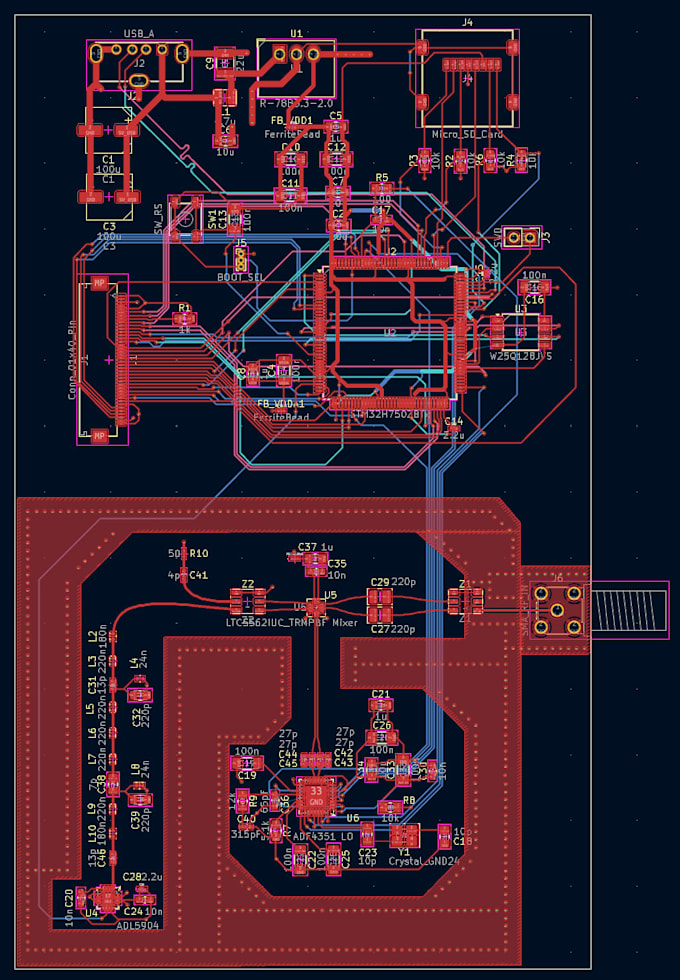
I will design a professional 2-layer PCB including schematic capture and a clean, manufacturable layout optimized for performance and cost efficiency. This package is ideal for small to medium complexity boards such as embedded systems, sensor boards, power modules, or custom controller designs.
This service includes:
Up to 2 PCB layers
Up to 50 components
Complete schematic design
Clean and optimized PCB layout
Basic signal and power integrity considerations
Bill of Materials (BOM)
Manufacturing-ready Gerber and drill files
Source design files
2 revisions
As an Electrical Engineer with strong background in circuit analysis, electronics, and system-level design, I focus on practical, production-ready solutions.