Browse categories
Explore
Fiverr Pro
English
$
USD
HTML CSS JAVA SCRIPT Django
Level 1
Has met certain performance criteria and shows strong potential in the marketplace.
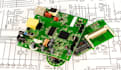
I provide professional PCB design, PCB layout, and circuit design services tailored to your project requirements. I work with EasyEDA, KiCad, and Altium Designer to deliver high-quality, manufacturable PCB files.
My services include schematic design, single-layer to multi-layer PCB layout, component placement, routing, design rule checks (DRC), and fabrication-ready outputs such as Gerber files, BOM, and pick-and-place files.
Whether you need a custom electronic circuit, PCB redesign, or optimization for manufacturing, I focus on clean layouts, signal integrity, and industry standards to ensure reliable performance.
I communicate clearly, deliver on time, and support you until your design is ready for production.

Specialization:
Circuit design
•
Schematics
•
Layout
•
Footprint
•
Gerber
File format:
Gerber
•
STEP
•
VRML
•
BRD
•
SCH
Software:
Altium Designer
•
Eagle CAD
•
EasyEDA
•
KiCad
•
LabVIEW
•
Proteus
Interface:
HDMI
•
I2S
•
TDM
•
UART
•
I2C
•
PCIe
•
Wi-Fi
•
BT
•
LTE
•
Ethernet
What information do you need to start the PCB design?
I need your circuit requirements, schematic (if available), board size, layer count, preferred software, and manufacturing constraints. If you don’t have everything, I can help you define it.
Which PCB design software do you use?
I work with EasyEDA, KiCad, and Altium Designer, depending on your project needs and preference.
Can you design the circuit and schematic from scratch?
Yes. I can design the complete circuit and schematic based on your idea, datasheet, or functional requirements.
Do you provide Gerber and manufacturing files?
Yes. I provide Gerber files, drill files, BOM, and pick-and-place files ready for PCB fabrication and assembly.


