Browse categories
Explore
Fiverr Pro
English
$
USD
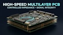
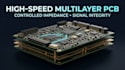
professional high speed multilayer RF PCB
HELLO AND WELCOME TO MY GIG!!!
Are you developing advanced electronic hardware that requires high speed signal routing, multilayer PCB engineering, controlled impedance, and reliable signal integrity?
I provide PCB engineering services for high-speed digital systems, embedded electronics, RF communication hardware, and complex electronic products. My approach focuses on routing discipline, stack-up planning, grounding strategy, component placement, and manufacturing requirements.
WHAT I OFFER
WHY WORK WITH ME?
I focus on understanding your board requirements before selecting the appropriate routing and layer strategy. I prioritize organized project files, clear communication, practical manufacturing considerations, and careful review of critical signal paths.