Browse categories
Explore
Fiverr Pro
English
$
USD
PCB Design, Reverse Engineering, Arduino And RF Antenna Specialist
Are you looking for a professional RF PCB and antenna design for a wireless electronics project?
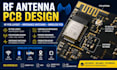
I will design an RF antenna PCB, RF PCB layout, controlled-impedance layout, antenna matching network, and wireless PCB according to your project requirements.
My services include:
I can work from your schematic, block diagram, existing PCB, reference design, datasheet, component selection, or project requirements.
My focus is clean RF layout, proper component placement, practical routing, grounding, signal integrity, and manufacturable PCB design.
Please contact me before ordering so I can review your frequency range, antenna type, board dimensions, wireless technology, stack-up requirements, and project specifications.

File format:
Gerber
•
STEP
•
Software:
EasyEDA
•
Fusion 360
•
KiCad
•
AutoCAD
•
SolidWorks
Interface:
NB-IoT
Do you provide RF simulation?
RF simulation depends on the project and the simulation software required. Please contact me before ordering so I can confirm whether your project requires simulation and what tools are appropriate.
Can you work with ESP32 or other wireless modules?
Yes. I can integrate RF/wireless modules such as ESP32 and other suitable modules into the PCB design.
What wireless technologies can you work with?
I can work with wireless applications such as WiFi, BLE, LoRa, GPS/GNSS, RF modules, IoT devices, and other wireless communication systems, depending on the project requirements.
Can you design impedance matching circuits?
Yes. I can implement RF matching networks and impedance-controlled PCB routing based on your RF design requirements and component specifications.
Can you design RF PCB layouts?
Yes. I can create RF PCB layouts with appropriate component placement, RF routing, grounding, and controlled-impedance considerations.
Can you design a PCB antenna?
Yes. I can design PCB antennas according to the required wireless frequency, board dimensions, application requirements, and available components.
