Browse categories
English
$
USD
Connect to your AI
PCB Designer, Altium Designer, Embedded Hardware
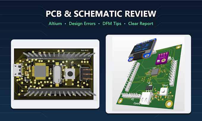
Not sure your PCB is ready for manufacturing? I will check your Altium schematic and PCB layout and send you a clear report of the problems I find and how to fix them.
What I check:
What you get:
Best for 2-layer boards made in Altium Designer (up to ~50 components). Please send me your project files (.PrjPcb, .SchDoc, .PcbDoc) before ordering so I can confirm the scope.

Specialization:
Schematics
•
Layout
•
Analysis
File format:
Gerber
•
•
Pcbdoc
Software:
Altium Designer
Interface:
UART
•
USB
•
SPI
•
I2C
Do you also fix the problems you find?
This gig is a review with a clear report. If you want me to apply the fixes in your Altium project too, message me and I will send a custom offer.
Can you review KiCad or EasyEDA projects?
I work in Altium Designer. For other tools, please send PDF exports of the schematic and Gerber files, and I will review those.
