Browse categories
Explore
Fiverr Pro
English
$
USD
electrical engineering
Struggling with unstable RF signals, poor antenna range, or failed IoT prototypes? Weak PCB design is often the hidden cause of performance loss.
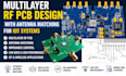
I will design multilayer RF PCB with precise antenna matching for reliable IoT wireless performance, ensuring strong signal integrity and manufacturable layouts.
What I offer:
Tools: Altium Designer, KiCad, ADS (RF analysis concepts)
Why choose me:
I focus on real RF engineering principles, not just layout. Every design is optimized for performance, reliability, and real-world manufacturing success.
You can message me before ordering to confirm requirements and avoid mistakes. This ensures your project is properly defined before we start.
Hi, Im Ben lets build your RF system the right way.

What do you need from me to start the RF PCB design?
I need your circuit details, frequency range, board size, layer preference, and antenna requirements (if any). If you’re unsure, I can help you define everything before starting.
Do you provide revision if something needs adjustment?
Yes, revisions are included depending on your package. I ensure the design meets RF performance expectations and manufacturing requirements before final delivery.
Will I receive production-ready files for manufacturing?
Yes. You will receive full production files including Gerbers, BOM, and Pick & Place files, fully ready for PCB fabrication and assembly.


