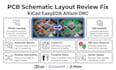
I will review fix pcb schematic layout kicad easyeda altium drc

United Kingdom

I speak English, German, Spanish, French, Italian

ELECTRICAL ENGINEER

Hello, I’m Benjamin Lewis, a professional PCB Design Engineer specializing in high-quality circuit board design and manufacturing files. I create clean, efficient, and production-ready PCB designs f...
About this Gig

I will review and fix your PCB schematic and layout using KiCad, EasyEDA, or Altium Designer.


If your board has errors, DRC issues, routing problems, grounding faults, or manufacturing risks, I will analyze the design and correct it for reliable performance and fabrication readiness.


Avoid costly manufacturing mistakes. Get your PCB verified and optimized before production.


What I Offer:

  • PCB Schematic Review
  • PCB Layout Review
  • DRC Error Fix
  • ERC Check
  • Routing Optimization
  • Component Placement Fix
  • Ground Plane Optimization
  • Trace Width Correction
  • Clearance Adjustment
  • Footprint Verification
  • Multilayer PCB Review
  • KiCad Support
  • EasyEDA Support
  • Altium Designer Support
  • Manufacturing Optimization


What You Will Get:

  • Detailed design review report
  • Fixed schematic files
  • Corrected PCB layout
  • DRC clean design
  • Improved routing structure
  • Updated Gerber files if required
  • Optimization suggestions


Contact me now to place your order!

Specialization:

Circuit design

Schematics

Layout

Footprint

File format:

Gerber

STEP

VRML

SCH

PDF

Software:

Altium Designer

Eagle CAD

EasyEDA

KiCad

AutoCAD

Arduino

Interface:

HDMI

MIPI DSI/CSI

I2S

TDM

UART

USB

SPI

I2C

SDIO

PCIe

BT