Browse categories
Explore
Fiverr Pro
English
$
USD
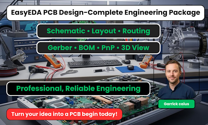
Turning circuit concepts into reliable, high performance PCB solutions
Hi! Im Garrick Caius, an Electrical Engineering graduate with 7+ years of experience turning concepts into functional, manufacturable electronics. I work in EasyEDA, designing PCBs that aren't just technically solid they're clean, reliable, cost efficient, and ready for assembly without the headaches.
I believe great hardware should be thoughtfully crafted, not rushed. Thats why I take time to understand your project, your goals, and the details that matter most. Whether its reducing the board size, cutting down costs, improving routing, or ensuring your design passes smoothly from prototype to production, I'm here to help you build something you're proud of.
Here's what you can expect from working with me:
Whether you're creating a new product, upgrading an existing circuit, or exploring an innovative idea, I'm here to bring your electronics vision to life one smart design at a time
message me now to get started


Specialization:
Circuit design
•
Schematics
•
Layout
•
Footprint
•
Gerber
File format:
Gerber
•
STEP
•
SCH
•
3DS
•
Software:
Altium Designer
•
Eagle CAD
•
EasyEDA
•
KiCad