Browse categories
English
$
USD
Connect to your AI
Electrical Engineering services by a TUe MSc student specializing in RF, FPGA,
Before you send your PCB to fab, let me check it for mistakes that could cost you time and money.
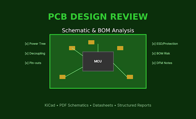
What I review:
Schematic correctness (pin assignments, net names, values)
Power distribution and decoupling
Component selection and BOM health
Layout issues (routing, clearances, planes)
Datasheet compliance
ESD and protection circuits
DFM concerns (manufacturability)
Deliverable:
A structured PDF report listing every finding with:
- Issue description
- Location (reference designator / net)
- Severity (critical / major / minor / suggestion)
- Recommended fix
Tools:
I work with KiCad files natively. Also accept Altium/Eagle exports, PDFs, or Gerbers + schematic images.
Background:
EE student at TU Eindhoven with coursework in analog, RF, and power electronics.
Note: This is a design review service, not a certification. I help you find issues final responsibility remains with you.

What file formats do you accept?
KiCad projects preferred. Also PDF schematics, Gerbers, Altium/Eagle exports, or clear images.
Do you do layout design or just review?
This gig is review-only. I check your work and suggest improvements.
What if you find critical issues?
I'll flag them prominently in the report with clear fix recommendations.
Can you review high-speed or RF boards?
I can review general layout and flag obvious issues. For detailed SI/PI analysis, specialized tools are needed.
How detailed is the report?
Every issue is documented with location, severity, and recommendation. Standard/Premium include annotated screenshots.
Is this a certification?
No — I provide design feedback, not compliance certification. You retain full responsibility for the design.
