Browse categories
Explore
Fiverr Pro
English
$
USD
Electronics Engineer PCB Design ESP32 Arduino IoT Expert
Hi,
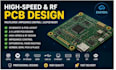
Looking for a professional PCB designer for high-speed or RF projects? You're in the right place.
I specialize in industry-standard PCB design with deep expertise in impedance control, signal integrity, and multilayer stackups (26 layers). From microcontrollers to RF circuits, I deliver manufacturing-ready designs optimized for JLCPCB.
What I offer:
Experience:
ESP32, STM32, FPGA, BGA, BLE, CAN, SPI, I2C, UART
Message me to discuss your project before ordering!

1. What software do you use for PCB design?
I use EasyEDA and industry-standard practices optimized for JLCPCB manufacturing.
2. Do you design high-speed and RF PCBs?
Yes, I specialize in impedance control, RF layouts, and high-speed interfaces like HDMI, USB, and Ethernet.
3. Will I get manufacturing-ready files?
Yes, you will receive Gerber, BOM, Pick & Place, and full fabrication files.
4. Can you handle multilayer PCB designs?
Yes, I design 2 to 6 layer PCBs with proper stackup and signal integrity.
5. Do you provide revisions?
Yes, revisions are included based on the package you choose.
