Browse categories
Explore
Fiverr Pro
English
$
USD
PCB and Embedded Systems
HELLO AND WELCOME TO MY GIG!!!
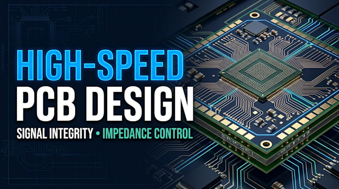
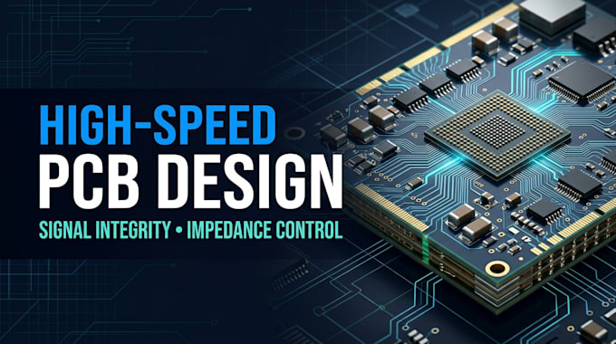
High-speed PCB design, signal integrity optimization, controlled-impedance routing, and multilayer hardware engineering for high-performance electronic systems. Specialized in differential pair routing, stackup planning, return path optimization, and noise-aware PCB layouts for reliable high-speed data transmission.
WHAT I OFFER;
WHY CHOOSE ME;
Kindly provide your interface specifications, data rates, stackup details, impedance targets, PCB dimensions, reference files, and manufacturing requirements.
MESSAGE ME NOW!!
What is high-speed PCB design?
High-speed PCB design focuses on routing signals where transmission-line effects, reflections, crosstalk, and return paths can affect signal quality and system reliability.
What is controlled impedance?
Controlled impedance means designing PCB traces to meet a specified impedance target based on the signal interface and the board's material stackup and geometry.
Can you route differential pairs?
Yes. Differential pairs can be routed with suitable spacing, reference planes, and length constraints based on the interface specifications.
Which high-speed interfaces can you support?
Depending on the project and design scope, these may include USB, DDR memory, PCIe, Ethernet, and other high-speed digital interfaces.
Can you design multilayer high-speed PCBs?
Yes. Layer planning, stackup requirements, routing constraints, and reference planes can be considered for multilayer designs.