Browse categories
Explore
Fiverr Pro
English
$
USD
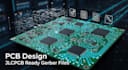
PCB DESIGN EXPERT
pcb design pcb layout gerber bom jlcpcb manufacturing ready pcb board.
This service focuses on creating pcb design files ready for fabrication with jlcpcb. The goal is to deliver clean schematic design and pcb layout that can be uploaded directly to the manufacturing platform without errors.
The workflow includes schematic preparation, pcb layout routing, and exporting gerber files compatible with jlcpcb fabrication standards.
Services include:
pcb schematic design
pcb layout routing
gerber file generation
bom file preparation
manufacturing ready pcb files
Compatible tools include:
kicad
easyeda
altium designer
This gig is suitable for:
prototype electronics
hardware startup projects
custom pcb boards
hobby electronics
The final files are structured so they can be directly uploaded to jlcpcb fabrication service for manufacturing.


Specialization:
Circuit design
•
Schematics
•
Layout
•
Analysis
•
Gerber
File format:
Gerber
•
STEP
•
VRML
•
ODB
Software:
Allegro
•
Cadence OrCAD
•
Eagle CAD
•
EasyEDA
•
KiCad
•
AutoCAD
What files will I receive
You will receive gerber files ready for jlcpcb manufacturing, schematic files, and source design files.
Can the PCB be uploaded directly to JLCPCB
Yes. The gerber files are exported according to jlcpcb fabrication requirements.
Can you create bom files
Yes, bom files can be provided for component sourcing.
Can you edit or fix my existing pcb
Yes, existing pcb layouts and schematics can be reviewed and improved.
Which software do you use
kicad easyeda and altium depending on the project needs.


