Browse categories
Explore
Fiverr Pro
English
$
USD
PCB DESIGN EXPERT
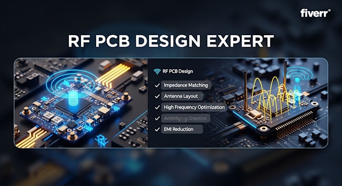
Are you struggling with RF PCB design issues like signal loss, noise, impedance mismatch, or poor antenna performance? High frequency circuits require precision and experience to avoid costly errors. I specialize in designing RF PCB layouts that ensure strong signal integrity and reliable performance.
I will design professional RF PCB layouts for wireless systems, IoT devices, antenna circuits, and high frequency applications. My designs focus on controlled impedance, proper grounding, and optimized trace routing to reduce interference and maximize efficiency.
You will get a clean, production ready PCB layout with proper stackup guidance, impedance matching, and RF routing techniques. I also consider EMI reduction, isolation, and component placement for best performance.
I work with tools like KiCad, Altium, and EasyEDA.
Perfect for engineers, startups, and developers building wireless products. Message me before ordering to review your requirements and ensure the best solution.


Specialization:
Circuit design
•
Schematics
•
Layout
•
Gerber
File format:
Gerber
•
STEP
Interface:
I2S
•
UART
•
SPI
•
I2C
•
SDIO
•
Ethernet
Can you design RF PCB for high frequency applications?
Yes, I specialize in high frequency and RF circuit layouts.
Do you handle impedance matching?
Yes, I design controlled impedance traces for optimal signal flow.
Can you design antenna PCB layouts?
Yes, I support antenna integration and RF optimization.
Will the design be ready for manufacturing?
Yes, I provide production-ready files if required.
Which tools do you use?
KiCad, Altium Designer, EasyEDA, and more.