Browse categories
Explore
Fiverr Pro
English
$
USD
PCB Design Embedded Electronics Engineer
HELLO GREAT BUYER
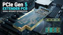
Need a reliable PCIe Gen 5 extender PCB with clean high speed signal performance?
I can design and optimize your PCIe Gen 5 extender, riser, or breakout PCB with careful attention to signal integrity, controlled impedance, differential pair routing, and high speed layout requirements. I work from your schematic, mechanical constraints, and electrical specifications to create a clean, manufacturable PCB layout.
WHAT I PROVIDE
WORKFLOW
Send your schematic, connector details, board dimensions, stackup, and specifications to get started.


What information do you need to start?
PCIe generation, connector details, board dimensions, layer preference, schematic and target stackup.
Can you design PCIe Gen 5 differential pairs?
Yes. I can handle controlled impedance, pair routing, length matching and topology requirements.
Do you optimize signal integrity?
Yes. I review routing, impedance, vias, return paths, crosstalk risks and other high-speed constraints.
Can you work with my existing PCB design?
Yes. I can review and optimize an existing PCIe layout or develop the extender from your schematic.
Which PCB software do you use?
I can work with professional PCB design environments such as Altium Designer and KiCad.
Do you provide manufacturing files?
Yes. Depending on the package, I can provide Gerbers, drill files, BOM, pick-and-place and source files.


