Browse categories
Explore
Fiverr Pro
English
$
USD
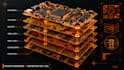
[ SYSTEM RUN: HARDWARE DECONSTRUCTION & SCHEMA RECOVERY ]
We execute advanced physical-to-digital hardware extraction, transforming legacy printed circuit board assemblies, bare copper layers, or high-resolution x-ray datasets back into fully editable, production-grade schematic diagrams and CAD layout databases.
// REVERSE ENGINEERING PIPELINE EXECUTED:
// DESTINATION PLATFORM DELIVERABLES:
Reconstructed hardware assets are compiled natively into fully layered project source folders using Altium Designer, Cadence Allegro, or KiCad workflows.
[ INTAKE_PROTOCOL ] -> Please initialize a direct message and transmit clear macro imagery of the board top/bottom layers alongside chip part numbers prior to order initialization.

Specialization:
Circuit design
•
Schematics
•
Other
File format:
Gerber
•
•
Pcbdoc
Software:
Altium Designer
•
KiCad
•
Arduino
Interface:
HDMI
•
PCIe
•
Other
Can you reverse engineer multi-layer boards without the original manufacturing Gerber files?
• Yes. For simple 2-layer boards, high-resolution top/bottom photography is sufficient. For multi-layer structures (4+ layers), we utilize non-destructive x-ray imaging layout maps or layer-by-layer delamination data to accurately track internal copper traces.
