Browse categories
Explore
Fiverr Pro
English
$
USD
[ TECHNICAL SPECIFICATION: PCB DFM CORRECTIONS & MANUFACTURING RESCUE ]
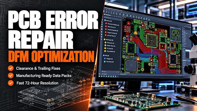
We provide rapid, high-precision structural design updates and Design for Manufacturing (DFM) calibrations to resolve manufacturing rejections, trace clearance failures, and netlist errors. We manually audit and repair layout layer data sheets to clear production bottlenecks before physical assembly deployment.
1. CRITICAL DESIGN REPAIRS PERFORMED:
2. PLATFORM WORKFLOWS SUPPORTED:
Layout files are corrected natively in Altium Designer, Cadence Allegro, or KiCad based on your strict design rules.
Please message us with your fabrication house error report and CAD layout files before ordering so we can verify the complexity of the design rule failure first!

Specialization:
Layout
•
Analysis
•
Gerber
File format:
Gerber
•
•
Pcbdoc
Software:
Altium Designer
•
Eagle CAD
•
EasyEDA
•
KiCad
•
PLECS
•
Arduino
Interface:
HDMI
•
USB
•
Other
What do you require to begin fixing the fabrication errors?
• We require your native layout database files along with the exact technical feedback sheet or redline report provided by your chosen PCB manufacturing house detailing the specific clearance errors.
