Browse categories
Explore
Fiverr Pro
English
$
USD
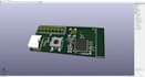
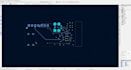
RF PCB Design, High Frequency Layout and Antenna Integration
Need professional RF PCB design for your wireless or high-frequency electronics project?
I provide RF PCB layout, antenna integration, and controlled-impedance routing for wireless devices, RF modules, and custom electronic products.
MY RF PCB DESIGN SERVICES:
WHY CHOOSE MY SERVICE?
I focus on clean PCB layouts, practical engineering requirements, organized des1gn files, and clear communication throughout your project.
Each design is approached according to its frequency requirements, board dimensions, components, and manufacturing constraints.
Whether you need a custom RF circuit board, wireless PCB layout, antenna integration, or impedance-controlled PCB routing, I can help define a suitable design workflow.
PLEASE CONTACT ME BEFORE ORDERING to discuss your project