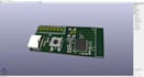
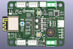
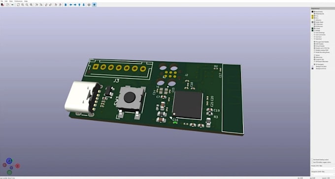
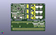
I will design rf pcb layout, antenna integration, impedance control and wifi pcb

United Kingdom

I speak English, German, Spanish, French, Italian, Portuguese

RF PCB Design, High Frequency Layout and Antenna Integration

I specialize in RF PCB design, high frequency PCB layout, antenna integration, and controlled-impedance routing for wireless and electronic devices. I provide PCB layout, RF circuit design, schemati...
About this Gig

Need professional RF PCB layout, Wi-Fi PCB design, antenna integration, and controlled impedance routing for your wireless electronics project?


I provide custom RF PCB design services for Wi-Fi devices, wireless modules, and high-frequency electronic products.


WHAT I OFFER:

  • RF PCB layout and high-frequency PCB routing
  • Wi-Fi PCB design and wireless module integration
  • Antenna placement and integration
  • Controlled impedance routing and transmission-line layout
  • Component placement, grounding, and routing optimization
  • RF schematic review and PCB design checks
  • Design for Manufacturing (DFM) review


WHAT I DELIVER:

  • Gerber and drill files
  • Bill of Materials (BOM)
  • PCB layout and schematic files, as agreed
  • PDF documentation
  • 3D STEP files, where applicable


SOFTWARE USED:

Altium Designer, KiCad, CST Studio Suite, LTspice, Cadence OrCAD, and EasyEDA, depending on project needs.


Whether you need a Wi-Fi RF PCB, antenna-integrated circuit board, wireless hardware layout, or impedance-controlled PCB routing, I focus on clean layouts and manufacturing-ready deliverables.


Contact me now
Specialization:

Circuit design

•

Schematics

•

Layout

•

Footprint

File format:

Gerber

•

STEP

•

SCH

•

PDF

•

Pcbdoc

Software:

Altium Designer

•

Cadence OrCAD

•

EasyEDA

•

KiCad

•

LTspice

Interface:

MIPI DSI/CSI

•

UART

•

USB

•

SPI

•

I2C

•

SDIO

•

Wi-Fi

•

BT

•

GSM/GPRS

•

LTE