Browse categories
Explore
Fiverr Pro
English
$
USD


Are you designing a consumer electronic device for mass production but don't know if your CAD design will work in an injection mold? Are you facing expensive tooling quotes because of design issues?
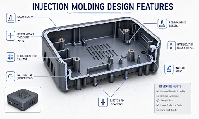
I specialize in injection molding CAD design for consumer electronics using SolidWorks. I create production-ready plastic housings, enclosures, and components optimized for injection molding with proper draft angles, wall thickness, ribs, and parting lines that manufacturers can actually mold.
Services included:
Device features:
Ready for production? Let's design it right
Please inform the freelancer of any preferences or concerns regarding the use of AI tools in the completion and/or delivery of your order.
Consumer Electronics CAD Engineer, SolidWorks and Injection Molding
Languages
What makes electronics enclosure design different from other injection molded products?
Electronics enclosures require extreme precision (±0.1-0.2mm tolerances) for PCB fit, precise alignment of buttons/ports to internal components, proper cable routing, EMI shielding considerations, heat dissipation features, and assembly design that protects sensitive electronics.
How do you determine the optimal wall thickness?
For consumer electronics, I typically design 1.5-2.5mm wall thickness balancing strength, moldability, and material cost. Thinner walls (1.2-1.5mm) reduce material and cooling time but require careful rib reinforcement. Thicker walls (2.5-3mm) are stronger but increase cycle time and warping risk.
What is a "parting line" and why does placement matter?
The parting line is where the two mold halves meet, creating a visible seam on your product. Poor placement puts this seam on the front face (ugly). I strategically place parting lines on edges, back surfaces, or natural product divisions so they're invisible from normal viewing angles.
What are "gate locations" and why do they matter?
Gates are where molten plastic enters the mold cavity. Gate location affects: visible gate marks (aesthetic issue), weld lines (weak points where plastic flows meet), warping (uneven cooling), and fill patterns.
How do I know the design will actually work in production?
The Standard package includes DFM (Design for Manufacturing) analysis identifying all potential molding issues before tooling. The Premium package includes detailed mold feasibility report with gate simulation, fill analysis, and manufacturability assessment.