Browse categories
Explore
Fiverr Pro
English
$
USD
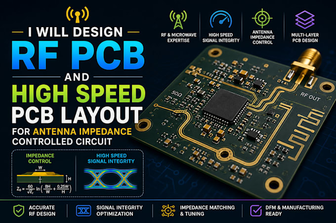
RF circuit designers often face issues with impedance mismatches and parasitic elements causing signal integrity problems. I specialize in designing and laying out RF PCBs and high-speed layouts precisely, ensuring optimal performance for your antenna circuits. I will deliver high-quality des.igns that minimize signal reflection and losses, enhancing overall circuit function.
What I Will Provide:
- RF PCB design for specified frequency
- High-speed layout optimization
- Impedance-controlled circuit de sign
- Reliable Gerber files
- Bill of Materials (BOM)
- Design rule verification
- Simulation reports
Why Choose Me:
I ensure signal integrity with precise impedance matching techniques, catching design issues others miss. My disciplined process results in robust circuit desi.gns that perform as intended.
Let's Get Started:
Please share your de-sign requirements and any specs to begin the design process.

Specialization:
Circuit design
•
Layout
•
Simulations
•
Gerber
File format:
Gerber
•
BRD
•
SCH
Software:
Altium Designer
•
Cadence OrCAD
•
KiCad
Interface:
USB
•
Ethernet
How do you ensure impedance control in the design?
Through careful trace width and spacing planning, and substrate material selection to maintain the required impedance.
Can you work with specific antenna types?
Yes, please provide your antenna specifications, and I'll optimize the layout accordingly.
What software tools do you use?
I primarily use Altium Designer and Cadence OrCAD for advanced PCB designs and simulations.
