Browse categories
English
$
USD
Connect to your AI
Are you looking for professional Semiconductor ATE Load Board PCB, IC testing hardware, or wafer test interface development for your next project?
I can help develop specialised electronic hardware for automated test equipment (ATE), semiconductor device testing, IC validation, and production testing applications.
Whether you need a custom load board, DUT interface PCB, wafer testing electronics, or a high density semiconductor test platform, I can help turn your technical requirements into a reliable PCB solution.
MY SERVICES INCLUDE:
MESSAGE ME BEFORE ORDERING so we can discuss your IC package, DUT requirements, test architecture, and expected deliverables.
What is a semiconductor ATE load board?
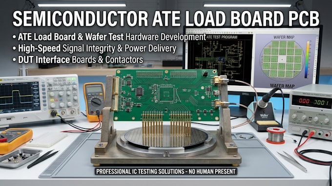
An ATE load board is an interface PCB that connects automated test equipment to a semiconductor device under test (DUT).
Can you develop custom ATE load boards?
Yes. I can develop custom load board layouts based on your device specifications, test requirements, and ATE platform.
Do you support wafer testing hardware?
Yes. I can help with wafer test interface electronics and related semiconductor testing boards.
Can you integrate DUT sockets?
Yes. I can support IC test socket, connector, and device interface integration based on the selected components.
Do you support multi site testing?
Yes. Multi site DUT architecture can be considered based on channel count, signal requirements, and available test resources.
Can you handle high density PCB layouts?
Yes. I can work on high density layouts, component placement, routing, and design rule verification according to the project specifications.
Can you work with existing ATE designs?
Yes. I can review existing schematics or PCB files for modifications, layout improvements, and troubleshooting.
Which PCB software do you use?
KiCad, Altium Designer, and EasyEDA, depending on project requirements.
Will I receive Gerber and BOM files?
Yes. Manufacturing outputs and documentation are included according to the selected package.
Can you guarantee that the load board will pass semiconductor production testing?
Production qualification depends on the ATE platform, DUT specifications, test program, and physical validation. I can provide PCB development and agreed design checks, but production performance must be verified through testing.
