Browse categories
Explore
Fiverr Pro
English
$
USD
iot product PCB Design, Product Design, PCB Layout, CAD and Enclosure Expert
Are you building a smart home device or wearable product, but designing a reliable LED lighting sensor PCB layout can be complex. IoT systems require precise PCB design for correct sensor behavior, power efficiency, and stable performance.
Without professional PCB des!gn, you may face issues like unstable sensor readings, poor LED performance, power inefficiency or complete system failure during prototyping or manufacturing. Many smart device projects fail due to weak PCB architecture and poor IoT integration.
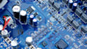
I will help you design a professional IoT LED sensor PCB layout for smart home devices and wearable electronics, ensuring your product is optimized for performance, reliability & manufacturing.
SERVICES I OFFER:
Send your idea, sketch, or requirements and lets build a reliable IoT PCB that Works!


What do you need to start my IoT PCB design project?
I need your idea description, circuit requirements, sensor details, LED function, reference images, sketches, or any existing schematic. Even a rough concept is enough to begin your IoT PCB design.
Can you design PCB for smart home and wearable devices?
Yes, I specialize in IoT PCB design including smart home device PCB layout, wearable electronics PCB design, and LED sensor integration with low-power optimization.
Will I receive Gerber files and BOM for manufacturing?
Yes. You will receive complete manufacturing files including PCB layout, schematic, Gerber files, and BOM (Bill of Materials) depending on your selected package.
Can you optimize PCB for low power and sensor accuracy?
Yes, I design IoT sensor PCB layouts with focus on low power consumption, stable LED control, and accurate sensor performance for real-world smart devices.
Do you support revisions if I need changes?
Yes, revisions are included depending on your package. I also ensure clear communication during PCB design for manufacturing to reduce the need for major revisions.


