Browse categories
Explore
Fiverr Pro
English
$
USD
Engineering Ideas, Designing Digital, Managing Success
Need a professional PCB designer to transform your circuit idea into a reliable, manufacturable board?
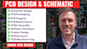
I specialize in high-quality PCB design, PCB layout, schematic capture, and electronic hardware development for startups, engineers, businesses, and makers. Whether you're developing a new product or improving an existing de-sign, I deliver optimized, production-ready PCB files with accuracy and attention to detail
Services include
I work with industry-standard tools such as Altium Designer, KiCad, EasyEDA, Eagle, and OrCAD to create clean, efficient, and fabrication-ready PCB de-sign that meet your project requirements
Why choose me?
Let's bring your product ideas to LIFE

What information do you need to start my PCB design project?
Please provide your circuit requirements, schematic (if available), component list, board dimensions, design constraints, and any special requirements. If you're still in the idea stage, I can help you plan the design.
Which PCB design software do you use?
I work with industry-standard tools, including Altium Designer, KiCad, EasyEDA, Eagle, and OrCAD, depending on your project requirements.
What files will I receive after the project is completed?
You will receive all necessary manufacturing files, including Gerber files, schematic files, PCB source files, BOM (Bill of Materials), Pick-and-Place files, and PDFs where required.
Can you design single-layer, double-layer, and multi-layer PCBs?
Yes. I design single-layer, double-layer, and multi-layer PCBs for a wide range of electronic applications.
Can you modify or improve an existing PCB design?
Absolutely. I can redesign, optimize, troubleshoot, or update your existing PCB layout to improve performance, reduce size, or prepare it for manufacturing.
Do you perform Design Rule Checks (DRC) before delivery?
Yes. Every PCB design is checked using Design Rule Checks (DRC) and Electrical Rule Checks (ERC) to help ensure it meets manufacturing standards.
Do you sign an NDA or keep my project confidential?Do you sign an NDA or keep my project confidential?
Yes. I respect client confidentiality and am happy to work under a Non-Disclosure Agreement (NDA) if required.
