Browse categories
Explore
Fiverr Pro
English
$
USD
United States
1 order completed
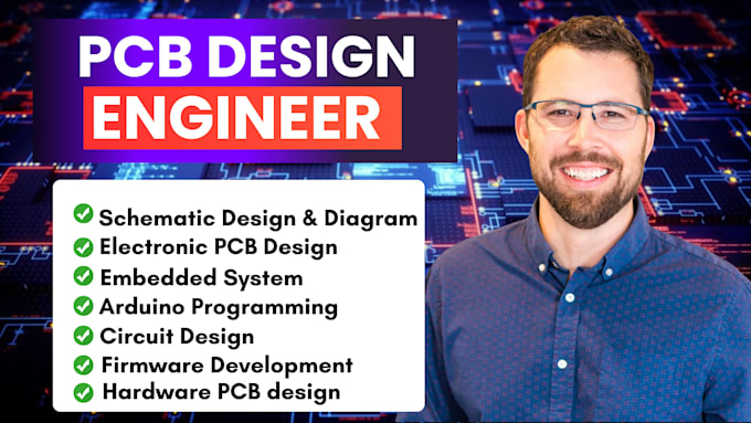
Reliable PCB Solutions from Concept to Fabrication
Looking for a reliable and skilled PCB designer to turn your idea into a production-ready circuit board? You're in the right place!
I am a professional PCB de-sign engineer with hands-on experience in IoT, robotics, consumer electronics, power electronics, and industrial automation. I specialize in creating accurate schematics, optimized PCB layouts, and manufacturer-ready files that meet industry standards
Using industry-leading EDA tools, I ensure high performance, signal integrity, and cost-effective de-sign from concept to final fabrication
What I Offer:
Design Tools
Altium Designer | KiCad | EasyEDA | Autodesk Eagle | OrCAD | Allegro PCB Designer | Proteus
ORDER NOW!


What do you need to start my PCB project?
I need your schematic (if available), project requirements, board size, layer count, and preferred components. If no schematic exists, I can create one from your concept.
Can you design both the schematic and PCB layout?
Yes. I provide full PCB services including schematic capture, circuit validation, and production-ready PCB layout.
Do you handle multilayer or high-speed PCBs?
Absolutely. I can design single-layer, double-layer, and multilayer boards, including high-speed circuits with controlled impedance and EMI/EMC considerations.
Can you optimize an existing PCB?
Yes. I can review and improve layouts for signal integrity, thermal management, manufacturability, and performance.
Which software tools do you use?
Altium Designer, KiCad, EasyEDA, Autodesk Eagle, Fusion 360 Electronics, and other industry-standard PCB design tools.
Can you help with prototype testing or production guidance?
Yes. I provide consultation on fabrication, component sourcing, and PCB assembly to ensure successful prototyping and production.